Department of Diamond Electronics
Head of Department – Tarelkin SergeyDepartment of diamond electronics active in the field of electrical and optical properties of diamond and other semiconductor materials and devices on their base.
The department was organized in 2017 due to growing interest to diamond-based electronics.
Main research area
- Development of novel high-power and high-frequency radiation resistant diamond electronics.
- Basic and applied research of synthetic semiconducting (p- and n-type) monocrystalline diamond.
- Development of materials and devices for quantum electronics, photonics, acoustoelectroics and optoelectronics.
- Development of sensitive elements for radiation detectors (ionizing, UV and IR).
- Development of long-duty autonomous beta-voltaic power sources.
Investigation methods
- Electrical resistance and Hall effect measurements in the range from 0.1 mOhm to 200 GOhm in the temperature range from 1.8 to 1200 K and magnetic field up to 9 T. Optical excitation of free charge carriers can be used.
- Heat capacity and thermal conductivity measurements for solids in the temperature range from 1.8 to 400 K.
- Static electric characteristics measurements for diode and triode structures. Voltage range – from 1 nV to 400 V, current range – from 1 fA to 10 A.
- Investigation of nonequilibrium charge carriers’ relaxation and transport by measuring Hall effect under optical excitation.
- Investigation of nonequilibrium electron-hole pairs relaxation mechanisms and diffusion length defining. Electron beam induced current (EBIC) mapping with logarithmic contrast.
- Investigation of nonqulibrium charge carriers mobility by the time-of-flight (ToF) method.
Technological capabilities
- Magnetron sputtering of metal films with the thickness control in the range from 1 to 1000 nanometers.
- Deposition of oxide and nitride films (including high-k films) up to 2 microns thick by the reactive magnetron sputtering.
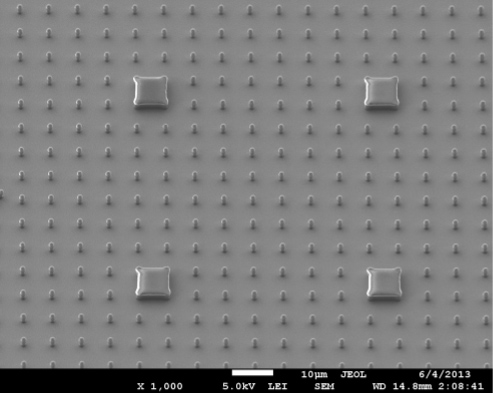
- Fabrication of metal and dielectric structures by classic and lift-off photolithography with up to 1 micrometer in-plane resolution.
- Formation of contact pads by up to 800 ° C annealing of metallic and intermetallic coatings in high vacuum (less than 10-6 torr).
- Electrical and opto-electrical measurements in a noise-free room (electromagnetic radiation attenuation factor > 40 dB).
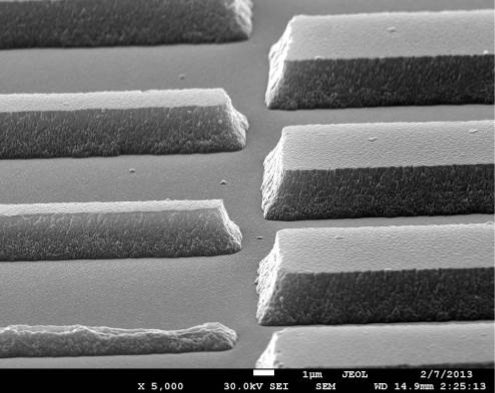
- Fabrication of complex profile microstructures with up to 20 micrometers height by the selective reactive ion etching (Ar, O2, CF4, SF6 etching mixtures) with metal and dielectric hardmasks on diamond and other semiconductor substrates.
- Fabrication of multilayer planar structures (in particular piezoelectric structures) by sequential “photolithography - film deposition” cycles with 100 nanometers alignment accuracy.
- We can work with non-conventional shape substrates with lateral size more than 3 millimeters.
 |
 |
 |
Primary results
1. Design and manufacturing technology of high-voltage high-frequency radiation resistive synthetic diamond Shottky diodes.
|
Diodes main characteristics: • reverse voltage • forward current • leak current at 1000 V • forward voltage drop at 5 A • operation temperature range • recovery time |
> 1000 V > 5 A < 100 uA < 100 mV от -60 – 250 °С < 10 ns |
 |
- A. Polyakov, N. Smirnov, S. Tarelkin, A. Govorkov, V. Bormashov, M. Kuznetsov, D. Teteruk, S. Buga, N. Kornilov, I.-H. Lee, Electrical Properties of Diamond Platinum Vertical Schottky Barrier Diodes, Materials Today: Proceedings. 3 (2016) S159–S164. doi:10.1016/j.matpr.2016.02.027.
- S. Tarelkin, V. Bormashov, S. Buga, A. Volkov, D. Teteruk, N. Kornilov, M. Kuznetsov, S. Terentiev, A. Golovanov, V. Blank, Power diamond vertical Schottky barrier diode with 10 A forward current, Phys. Status Solidi A. 212 (2015) 2621. doi:10.1002/pssa.201532213.
- V.D. Blank, V.S. Bormashov, S.A. Tarelkin, S.G. Buga, M.S. Kuznetsov, D.V. Teteruk, N.V. Kornilov, S.A. Terentiev, A.P. Volkov, Power high-voltage and fast response Schottky barrier diamond diodes, Diamond and Related Materials. (2015). doi:10.1016/j.diamond.2015.01.005.
- Д.В. Тетерук, С.А. Тарелкин, В.С. Бормашов, А.П. Волков, Н.В. Корнилов, С.А. Терентьев, Легирование алмаза, выращенного методом газофазного осаждения, Известия ВУЗов. Химия и химическая технология. 57 (2014) 56–58. (выпуск журнала)
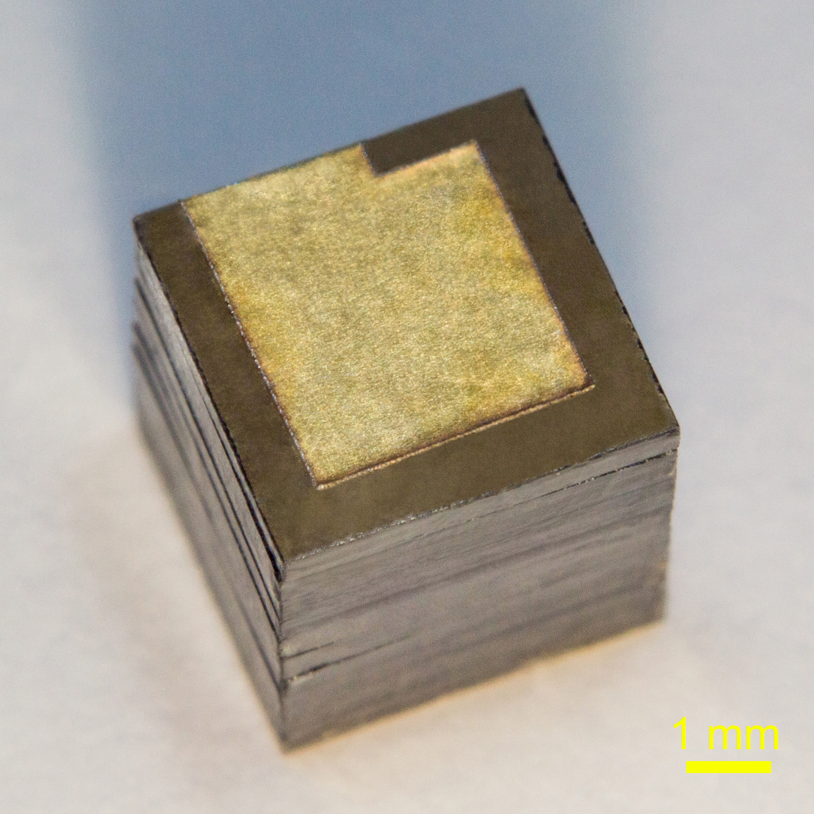
2. Technology of manufacturing ultrathin electronic grade diamond plates. The technique includes producing an ion-damaged layer under the surface of the diamond plate followed by electrochemical etching and detachment of thin plate. 15 um thickness at 5x5 mm2 sizes were achieved. These thin plates were used for design of Shottky diodes with high density of forward current.

- V.S. Bormashov, S.A. Terentiev, S.G. Buga, S.A. Tarelkin, A.P. Volkov, D.V. Teteruk, N.V. Kornilov, M.S. Kuznetsov, V.D. Blank, Thin large area vertical Schottky barrier diamond diodes with low on-resistance made by ion-beam assisted lift-off technique, Diamond & Related Materials. 75 (2017) 78–84. doi:http://dx.doi.org/10.1016/j.diamond.2017.02.006.
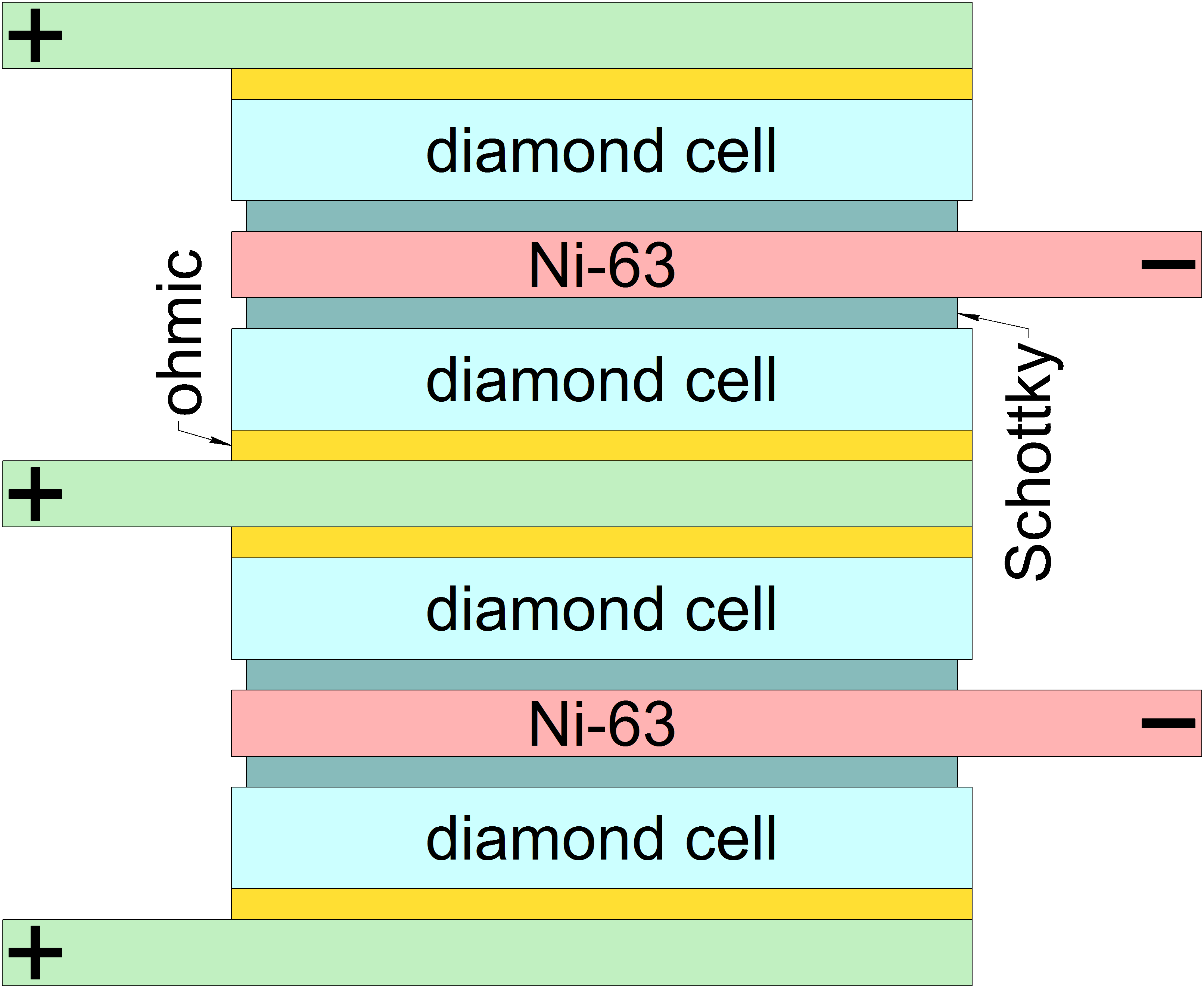
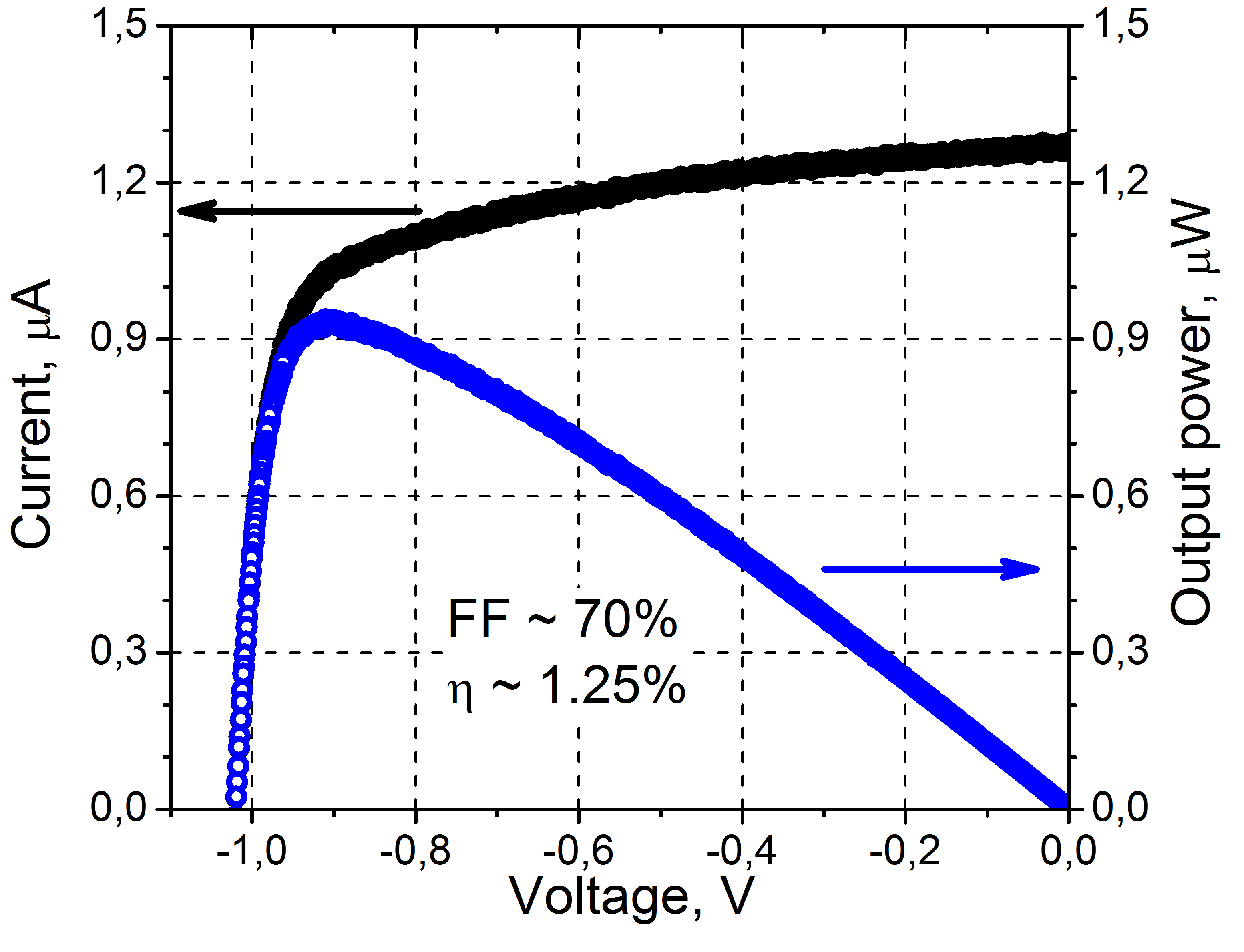
3. Autonomous radiation stimulated beta-voltaic batteries with more than 20 years lifetime were designed. For the first time in the world, the possibility of power density higher than 50 uW/cm3 in radiation stimulated batteries based on 63Ni was shown.
 |
 |
|
Assembly of 200 diamond power convertors and 100 63Ni sources |
Scheme of battery assembly |
|
 |
 |
|
IV curve (black) and dependence of active power on voltage (blue) for the battery |
Battery electrical load curve |
- V.S. Bormashov, S.Y. Troschiev, S.A. Tarelkin, A.P. Volkov, D.V. Teteruk, A.V. Golovanov, M.S. Kuznetsov, N.V. Kornilov, S.A. Terentiev, V.D. Blank, High power density nuclear battery prototype based on diamond Schottky diodes, Diamond and Related Materials. 84 (2018) 41–47. doi:10.1016/j.diamond.2018.03.006.
- S. Tarelkin, V. Bormashov, E. Korostylev, S. Troschiev, D. Teteruk, A. Golovanov, A. Volkov, N. Kornilov, M. Kuznetsov, D. Prikhodko, S. Buga, Comparative study of different metals for Schottky barrier diamond betavoltaic power converter by EBIC technique, Physica Status Solidi (A). (2016). doi:10.1002/pssa.201533060.
- А.В. Голованов, В.С. Бормашов, А.П. Волков, С.А. Тарелкин, С.Г. Буга, В.Д. Бланк, Создание развитой поверхности синтетического монокристалла алмаза для повышения удельной мощности бета-вольтаических источников питания на их основе, Известия ВУЗов. Химия и химическая технология. 59 (2016) 86–91. (выпуск журнала).
- V. Bormashov, S. Troschiev, A. Volkov, S. Tarelkin, E. Korostylev, A. Golovanov, M. Kuznetsov, D. Teteruk, N. Kornilov, S. Terentiev, S. Buga, V. Blank, Development of nuclear microbattery prototype based on Schottky barrier diamond diodes, Phys. Status Solidi A. 212 (2015) 2539. doi:10.1002/pssa.201532214.
4. Sensitive elements for high-speed neutron detectors were designed and are currently produced of synthetic diamond. At this moment, we produce detectors of two kinds of shape: shim with M#0.8 carving or disks with central electrode.
Sensitive elements – shims |
Sensitive elements – disks |
IV curve of the detector in the dark and under UV radiation |
- V.S. Bormashov, S.A. Tarelkin, N.V. Luparev, A.N. Kirichenko, M.S. Kuznetsov, S.A. Terentiev, V.D. Blank, M.A. Bublik, B.A. Zabolotko, V.V. Ivanov, E.V. Pozdnyakov, S.P. Martynenko, Natural and HPHT IIa diamonds as fast neutron detectors for inertial confinement fusion diagnostics, in: Haaselt University, Hasselt, Belgium, 2017: p. 113.
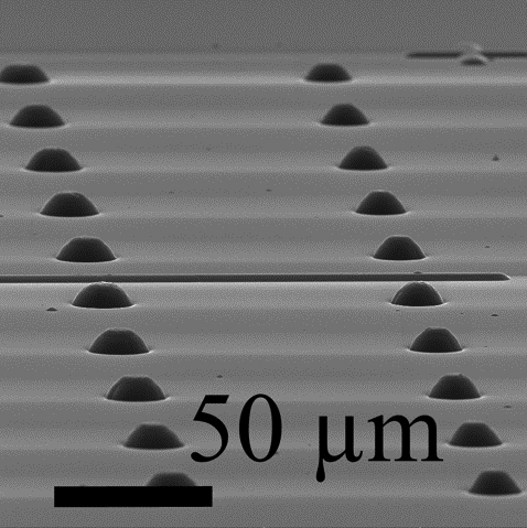
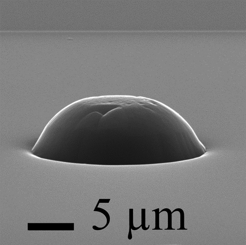
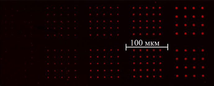
5. We designed the technology of single NV-centers formation in HPHT diamond plates and the technology of diamond solid immersion optical lenses (SIL) fabrication.
 |
 |
|
 |
 |
|
Formation of solid immersion optical lenses on diamond surface using grayscailing masks |
||
 |
 |
|
Mask for ion implantation, minimal hole diameter ~500 nm |
NV-centers photoluminescence intensity map (637 nm) |
|
- A.V. Golovanov, V.S. Bormashov, N.V. Luparev, S.A. Tarelkin, S.Y. Troschiev, S.G. Buga, V.D. Blank, Diamond Microstructuring by Deep Anisotropic Reactive Ion Etching, Physica Status Solidi (A). (2018) 1800273. doi:10.1002/pssa.201800273
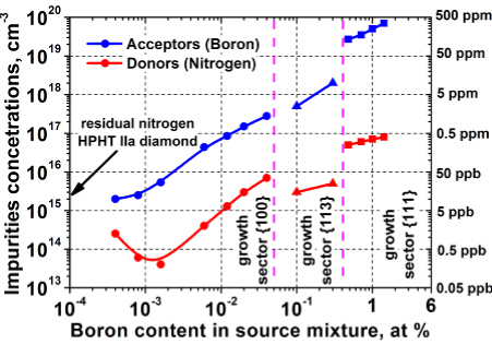
6. Electrical properties of boron-doped synthetic HPHT diamonds dependence on synthesis conditions was investigated. Optimal growth parameters for electronic applications were defined.
 |
 |
- В.С. Бормашов, С.А. Тарелкин, С.Г. Буга, А.П. Волков, А.В. Голованов, М.С. Кузнецов, Н.В. Корнилов, Д.В. Тетерук, С.А. Терентьев, В.Д. Бланк, Электрические свойства высококачественных синтетических монокристаллов алмаза, легированных бором, и диодов Шоттки на их основе, Заводская лаборатория. Диагностика материалов. 83 (2017) 36–42. (статья)
- V. Blank, S. Buga, V. Bormashov, V. Denisov, A. Kirichenko, V. Kulbachinskii, M. Kuznetsov, V. Kytin, G. Kytin, S. Tarelkin, S. Terentiev, Weak superconductivity in the surface layer of a bulk single-crystal boron-doped diamond, EPL (Europhysics Letters). 108 (2014) 67014. doi:10.1209/0295-5075/108/67014.
- V.S. Bormashov, S.A. Tarelkin, S.G. Buga, M.S. Kuznetsov, S.A. Terentiev, A.N. Semenov, V.D. Blank, Electrical properties of the high quality boron-doped synthetic single-crystal diamonds grown by the temperature gradient method, Diamond and Related Materials. 35 (2013) 19–23. doi:10.1016/j.diamond.2013.02.011.
- В.С. Бормашов, С.А. Тарелкин, М.С. Кузнецов, С.А. Терентьев, С.Г. Буга, Электрофизические свойства легированных бором синтетических монокристаллов алмаза, Наноиндустрия. 2012 (2012) 32–37.
- V.D. Blank, S.G. Buga, S.A. Terentiev, M.S. Kuznetsov, S.A. Nosukhin, A.V. Krechetov, V.A. Kul’bachinski, V.G. Kytin, G.A. Kytin, Low-temperature electrical conductivity of heavily boron-doped diamond single crystals, Phys. Sat. Sol. (B). 244 (2007) 413–417. doi:10.1002/pssb.200672526.
7. Technique of mechanical polishing, cleaning and following diamond plates control for obtaining smooth and clean surface for electronic applications was designed.
- M.A. Doronin, S.N. Polyakov, K.S. Kravchuk, S.P. Molchanov, A.A. Lomov, S.Yu. Troschiev, S.A. Terentiev, Limits of single crystal diamond surface mechanical polishing, Diamond and Related Materials. (2018). doi:10.1016/j.diamond.2018.05.016.
- E.V. Korostylev, V.S. Bormashov, S.A. Tarelkin, M.A. Doronin, Using electron backscatter diffraction to investigate the influence of mechanical polishing on the state of the surface of diamond, Journal of Surface Investigation: X-Ray, Synchrotron and Neutron Techniques. 11 (2017) 125–129. doi:10.1134/S1027451017010141.
- M.A. Doronin, K.V. Larionov, S.Yu. Troschiev, S.A. Terentiev, Dependence of Synthetic Diamond Wear Rate on Lattice Orientation at Traditional Mechanical Treatment, Journal of Surface Investigation: X-Ray, Synchrotron and Neutron Techniques. 11 (2017) 1192–1195. doi:10.1134/S1027451017060052.
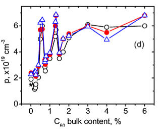
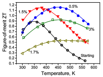
8. In collaboration with Department of Functional and Structural Nanomaterials, we designed and investigated new composite nanostructured thermoelectric materials based on alloy of Bi-Sb-Te with C60. We achieved 30-70% rise of thermoelectric figure of merit ZT in a wide temperature range. Effect of “resonance” C60 concentrations with up to 6 electrons capture per fullerene molecule was discovered.
 |
 |
|
Dependence of free charge carriers (holes) concentration on fullerene C60 content in alloy Bi0.5-Sb1-Te3-C60 |
Temperature dependencies of thermoelectric figure of merit ZT for Bi0.5-Sb1-Te3-C60 alloys at different C60 content |
- D.A. Ovsyannikov, M.Y. Popov, S.G. Buga, A.N. Kirichenko, S.A. Tarelkin, V.V. Aksenenkov, E.V. Tat’yanin, V.D. Blank, Transport properties of nanocomposite thermoelectric materials based on Si and Ge, Physics of the Solid State. 57 (2015) 605–612. doi:10.1134/S1063783415030208.
- M. Popov, S. Buga, P. Vysikaylo, P. Stepanov, V. Skok, V. Medvedev, E. Tatyanin, V. Denisov, A. Kirichenko, V. Aksenenkov, V. Blank, C60-doping of nanostructured Bi-Sb-Te thermoelectrics, Physica Status Solidi (A). 208 (2011) 2783–2789. doi:10.1002/pssa.201127075.
- V.D. Blank, S.G. Buga, V.A. Kulbachinskii, V.G. Kytin, V.V. Medvedev, M.Y. Popov, P.B. Stepanov, V.F. Skok, Thermoelectric properties of Bi0.5Sb1.5Te3/C60 nanocomposites, Physical Review B. 86 (2012). doi:10.1103/PhysRevB.86.075426.
9. New metastable phases of topological isolators Sb2Te3 and Bi2Se3 were synthesized and investigated. The synthesis technique is quenching after high-pressure-high-temperature treatment. Transition into low-dimension superconductive state (weak superconductivity) in the new Sb2Te3 phase was found. The critical superconductivity temperature is 2 K. We observed an effect of linear positive magnetoresistance at strong fields 2 – 9 T in low temperature range. At room and lower temperatures, the zero-field paramagnetic cusp in susceptibility was observed. Both effects indicate the topological isolator (semimetal) state.
- V.A. Kulbachinskii, S.G. Buga, N.R. Serebryanaya, N.S. Perov, V.G. Kytin, S.A. Tarelkin, R.H. Bagramov, N.N. Eliseev, V.D. Blank, Superconductivity, Magnetoresistance, Magnetic Anomaly and Crystal Structure of New Phases of Topological Insulators Bi2Se3 and Sb2Te3, Journal of Physics: Conference Series. 969 (2018) 012152. doi:10.1088/1742-6596/969/1/012152.
- N. Serebryanaya, E. Tatyanin, S. Buga, I. Kruglov, N. Lvova, V. Blank, Monoclinic structure and electrical properties of metastable Sb2Te3 and Bi0.4Sb1.6Te3 phases: Structure and properties of metastable Sb2Te3 and Bi0.4Sb1.6Te3 phases, Physica Status Solidi (B). 252 (2015) 267–273. doi:10.1002/pssb.201451241.
- S.G. Buga, V.A. Kulbachinskii, V.G. Kytin, G.A. Kytin, I.A. Kruglov, N.A. Lvova, N.S. Perov, N.R. Serebryanaya, S.A. Tarelkin, V.D. Blank, Superconductivity in bulk polycrystalline metastable phases of Sb2Te3 and Bi2Te3 quenched after high-pressure–high-temperature treatment, Chemical Physics Letters. 631–632 (2015) 97–102. doi:10.1016/j.cplett.2015.04.056.
- S.G. Buga, N.R. Serebryanaya, G.A. Dubitskiy, E.E. Semenova, V.V. Aksenenkov, V.D. Blank, Structure and electrical properties of Sb2Te3 and Bi0.4Sb1.6Te3 metastable phases obtained by HPHT treatment, High Pressure Research. 31 (2011) 86–90. doi:10.1080/08957959.2010.523422.
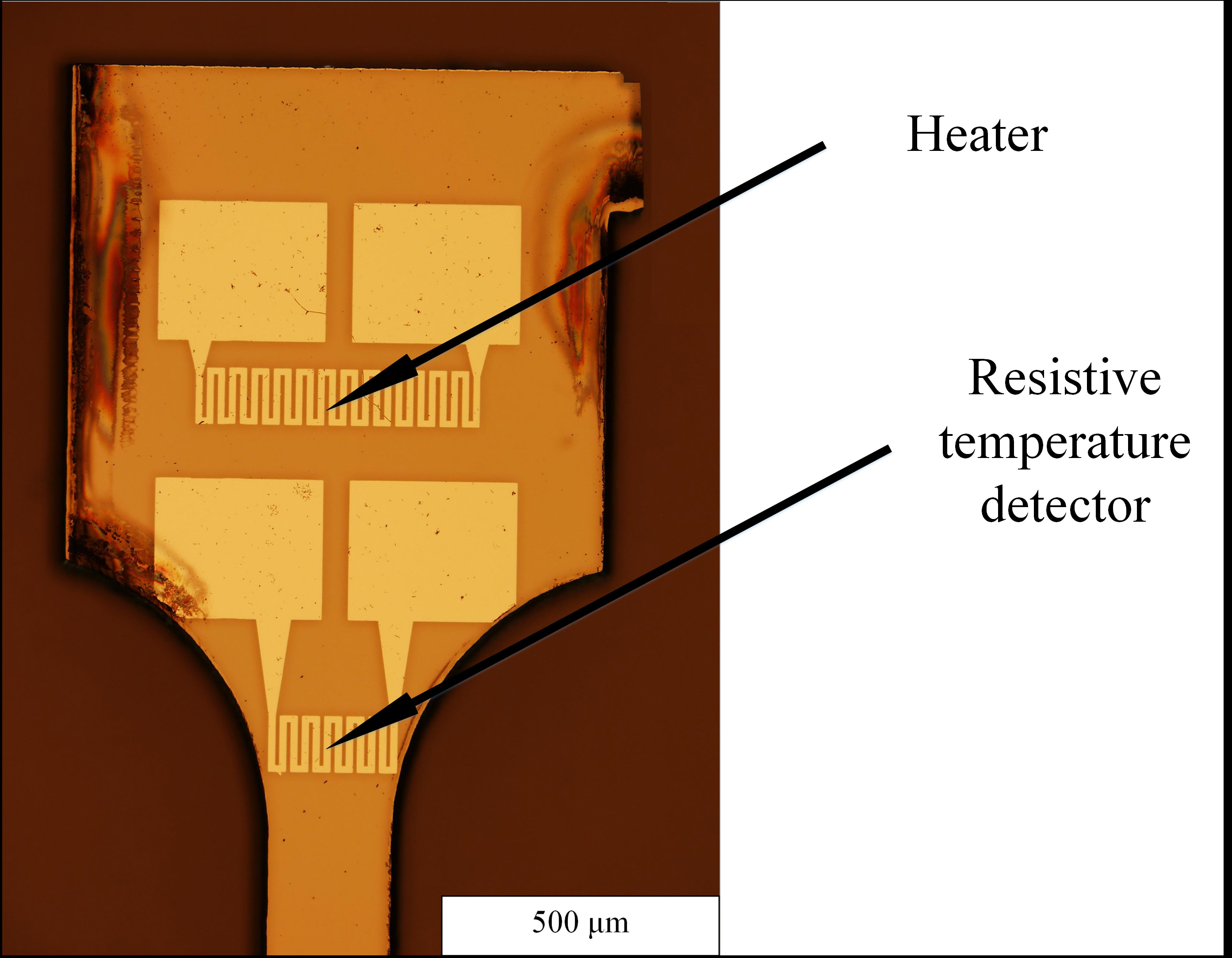
10. We designed methods for measuring heat capacity and extremely high thermal conductivity of diamond in the temperature range 2 – 400 K.
 |
 |
|
Diamond sample on a holder |
Heater and temperature detector on the sample |
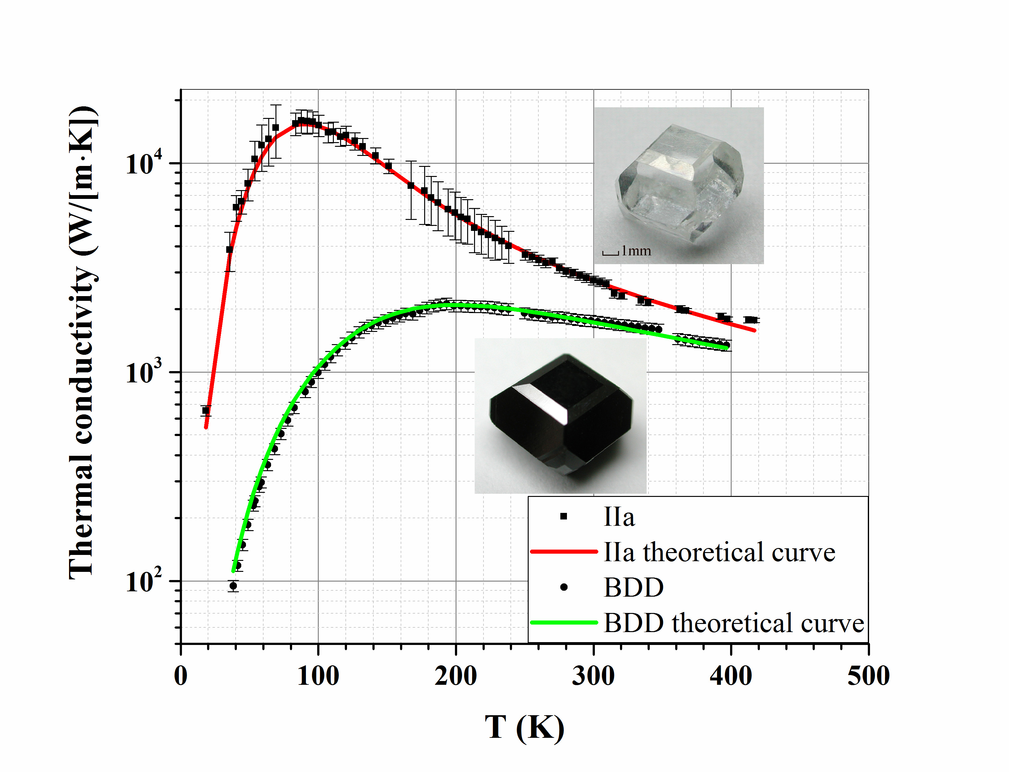 |
Measurement of thermal conductivity of pure IIa type and boron-doped IIb type diamonds |
- S. Tarelkin, V. Bormashov, M. Kuznetsov, S. Buga, S. Terentiev, D. Prikhodko, A. Golovanov, V. Blank, Heat capacity of bulk boron-doped single-crystal HPHT diamonds in the temperature range from 2 to 400 K, Journal of Superhard Materials. 38 (2016) 412–416. doi:10.3103/S1063457616060058.
- D. Prikhodko, S. Tarelkin, V. Bormashov, A. Golovanov, M. Kuznetsov, D. Teteruk, A. Volkov, S. Buga, Thermal conductivity of synthetic boron-doped single-crystal HPHT diamond from 20 to 400 K, MRS Communications. (2016) 1–6. doi:10.1557/mrc.2016.12.
Perspective electronics based on synthetic diamond
- High-power high-speed Shottky diodes
- High-power high-frequency field-effect transistors
- Autonomous long lifetime power sources (“atomic batteries”)
- Integral optical and optoelectronic schemes on diamond chip
- Devices for information quantum processing and transfer on color centers (NV, SiV)
- Room temperature MASERs and THz sources
- Sun-blind UV sensor including matrix detectors (spectral range < 250 nm)
- Dose detectors and matrix detectors for X-ray and γ radiation
- Spectrometric detectors of ionizing radiation with high energy resolution
- Counting sensors for measuring ionizing radiation flux density
- Sensitive elements of powermeters for laser radiation in kW range
- Superconductive sensors of IR radiation
- Temperature sensors in a wide range from 77 to 800 K
- Acoustoelectric filters, delay lines and resonators in microwave range
- Single- and broadband microwave generators
- Elements for optical RAM
Department staff publications (40 publications)
- A.V. Golovanov, V.S. Bormashov, N.V. Luparev, S.A. Tarelkin, S.Y. Troschiev, S.G. Buga, V.D. Blank, Diamond Microstructuring by Deep Anisotropic Reactive Ion Etching, Physica Status Solidi (A). (2018) 1800273. doi:10.1002/pssa.201800273
- V.S. Bormashov, S.Yu. Troschiev, S.A. Tarelkin, A.P. Volkov, D.V. Teteruk, A.V. Golovanov, M.S. Kuznetsov, N.V. Kornilov, S.A. Terentiev, V.D. Blank, High power density nuclear battery prototype based on diamond Schottky diodes, Diamond and Related Materials. 84 (2018) 41–47. doi:10.1016/j.diamond.2018.03.006.
- M.A. Doronin, S.N. Polyakov, K.S. Kravchuk, S.P. Molchanov, A.A. Lomov, S.Yu. Troschiev, S.A. Terentiev, Limits of single crystal diamond surface mechanical polishing, Diamond and Related Materials. (2018). doi:10.1016/j.diamond.2018.05.016.
- V.A. Kulbachinskii, S.G. Buga, N.R. Serebryanaya, N.S. Perov, V.G. Kytin, S.A. Tarelkin, R.H. Bagramov, N.N. Eliseev, V.D. Blank, Superconductivity, Magnetoresistance, Magnetic Anomaly and Crystal Structure of New Phases of Topological Insulators Bi2Se3 and Sb2Te3, Journal of Physics: Conference Series. 969 (2018) 012152. doi:10.1088/1742-6596/969/1/012152.
- V. Sadovoy, V. Blank, D. Teteruk, S. Terentiev, N. Kornilov, HPHT single crystal diamond type IIB growth sector influence on the secondary electron emission phenomenon, Journal of Surface Investigation: X-Ray, Synchrotron and Neutron Techniques. 11 (2017) 1101–1107. doi:10.1134/S1027451017050366.
- B.P. Sorokin, G.M. Kvashnin, A.S. Novoselov, V.S. Bormashov, A.V. Golovanov, S.I. Burkov, V.D. Blank, Excitation of hypersonic acoustic waves in diamond-based piezoelectric layered structure on the microwave frequencies up to 20 GHz, Ultrasonics. 78 (2017) 162–165. doi:10.1016/j.ultras.2017.01.014.
- S.A. Tarelkin, V.S. Bormashov, S.G. Pavlov, D.L. Kamenskyi, M.S. Kuznetsov, S.A. Terentiev, D.D. Prikhodko, A.S. Galkin, H.-W. Hübers, V.D. Blank, Evidence of linear Zeeman effect for infrared intracenter transitions in boron doped diamond in high magnetic fields, Diamond and Related Materials. 75 (2017) 52–57. doi:10.1016/j.diamond.2017.01.004.
- E.V. Korostylev, V.S. Bormashov, S.A. Tarelkin, M.A. Doronin, Using electron backscatter diffraction to investigate the influence of mechanical polishing on the state of the surface of diamond, Journal of Surface Investigation: X-Ray, Synchrotron and Neutron Techniques. 11 (2017) 125–129. doi:10.1134/S1027451017010141.
- M.A. Doronin, K.V. Larionov, S.Yu. Troschiev, S.A. Terentiev, Dependence of Synthetic Diamond Wear Rate on Lattice Orientation at Traditional Mechanical Treatment, Journal of Surface Investigation: X-Ray, Synchrotron and Neutron Techniques. 11 (2017) 1192–1195. doi:10.1134/S1027451017060052.
- V.S. Bormashov, S.A. Terentiev, S.G. Buga, S.A. Tarelkin, A.P. Volkov, D.V. Teteruk, N.V. Kornilov, M.S. Kuznetsov, V.D. Blank, Thin large area vertical Schottky barrier diamond diodes with low on-resistance made by ion-beam assisted lift-off technique, Diamond & Related Materials. 75 (2017) 78–84. doi:http://dx.doi.org/10.1016/j.diamond.2017.02.006.
- В.С. Бормашов, С.А. Тарелкин, С.Г. Буга, А.П. Волков, А.В. Голованов, М.С. Кузнецов, Н.В. Корнилов, Д.В. Тетерук, С.А. Терентьев, В.Д. Бланк, Электрические свойства высококачественных синтетических монокристаллов алмаза, легированных бором, и диодов Шоттки на их основе, Заводская лаборатория. Диагностика материалов. 83 (2017) 36–42. (сайт журнала).
- А.В. Голованов, В.С. Бормашов, А.П. Волков, С.А. Тарелкин, С.Г. Буга, В.Д. Бланк, Создание развитой поверхности синтетического монокристалла алмаза для повышения удельной мощности бета-вольтаических источников питания на их основе, Известия ВУЗов. Химия и химическая технология. 59 (2016) 86–91. (выпуск журнала).
- В.Ю. Садовой, В.Д. Бланк, С.А. Терентьев, С.Ю. Трощиев, Исследование влияния кристаллографического направления синтетического монокристалла алмаза на коэффициент вторичной электронной эмиссии, Известия ВУЗов. Химия и Химическая Технология. 59 (2016) 21–26. (выпуск журнала).
- S. Tarelkin, V. Bormashov, M. Kuznetsov, S. Buga, S. Terentiev, D. Prikhodko, A. Golovanov, V. Blank, Heat capacity of bulk boron-doped single-crystal HPHT diamonds in the temperature range from 2 to 400 K, Journal of Superhard Materials. 38 (2016) 412–416. doi:10.3103/S1063457616060058.
- Д.В. Тетерук, В.С. Бормашов, С.А. Тарелкин, Н.В. Корнилов, Н.В. Лупарев, А.Н. Кириченко, Подавление синтеза алмаза на торцевой поверхности подложки в процессе газофазного осаждения, Известия ВУЗов. Химия и химическая технология. 59 (2016) 64–68. (выпуск журнала).
- S. Tarelkin, V. Bormashov, E. Korostylev, S. Troschiev, D. Teteruk, A. Golovanov, A. Volkov, N. Kornilov, M. Kuznetsov, D. Prikhodko, S. Buga, Comparative study of different metals for Schottky barrier diamond betavoltaic power converter by EBIC technique, Physica Status Solidi (A). (2016). doi:10.1002/pssa.201533060.
- D. Prikhodko, S. Tarelkin, V. Bormashov, A. Golovanov, M. Kuznetsov, D. Teteruk, A. Volkov, S. Buga, Thermal conductivity of synthetic boron-doped single-crystal HPHT diamond from 20 to 400 K, MRS Communications. (2016) 1–6. doi:10.1557/mrc.2016.12.
- A. Polyakov, N. Smirnov, S. Tarelkin, A. Govorkov, V. Bormashov, M. Kuznetsov, D. Teteruk, S. Buga, N. Kornilov, I.-H. Lee, Electrical Properties of Diamond Platinum Vertical Schottky Barrier Diodes, Materials Today: Proceedings. 3 (2016) S159–S164. doi:10.1016/j.matpr.2016.02.027.
- S. Tarelkin, V. Bormashov, S. Buga, A. Volkov, D. Teteruk, N. Kornilov, M. Kuznetsov, S. Terentiev, A. Golovanov, V. Blank, Power diamond vertical Schottky barrier diode with 10 A forward current, Phys. Status Solidi A. 212 (2015) 2621. doi:10.1002/pssa.201532213.
- V. Bormashov, S. Troschiev, A. Volkov, S. Tarelkin, E. Korostylev, A. Golovanov, M. Kuznetsov, D. Teteruk, N. Kornilov, S. Terentiev, S. Buga, V. Blank, Development of nuclear microbattery prototype based on Schottky barrier diamond diodes, Phys. Status Solidi A. 212 (2015) 2539. doi:10.1002/pssa.201532214.
- S.G. Buga, V.A. Kulbachinskii, V.G. Kytin, G.A. Kytin, I.A. Kruglov, N.A. Lvova, N.S. Perov, N.R. Serebryanaya, S.A. Tarelkin, V.D. Blank, Superconductivity in bulk polycrystalline metastable phases of Sb2Te3 and Bi2Te3 quenched after high-pressure–high-temperature treatment, Chemical Physics Letters. 631–632 (2015) 97–102. doi:10.1016/j.cplett.2015.04.056.
- N. Serebryanaya, E. Tatyanin, S. Buga, I. Kruglov, N. Lvova, V. Blank, Monoclinic structure and electrical properties of metastable Sb2Te3 and Bi0.4Sb1.6Te3 phases: Structure and properties of metastable Sb2Te3 and Bi0.4Sb1.6Te3 phases, Physica Status Solidi (B). 252 (2015) 267–273. doi:10.1002/pssb.201451241.
- S.G. Buga, V.A. Kulbachinskii, V.G. Kytin, G.A. Kytin, I.A. Kruglov, N.A. Lvova, N.S. Perov, N.R. Serebryanaya, S.A. Tarelkin, V.D. Blank, Superconductivity in bulk polycrystalline metastable phases of Sb2Te3 and Bi2Te3 quenched after high-pressure–high-temperature treatment, Chemical Physics Letters. 631–632 (2015) 97–102. doi:10.1016/j.cplett.2015.04.056.
- V.D. Blank, V.S. Bormashov, S.A. Tarelkin, S.G. Buga, M.S. Kuznetsov, D.V. Teteruk, N.V. Kornilov, S.A. Terentiev, A.P. Volkov, Power high-voltage and fast response Schottky barrier diamond diodes, Diamond and Related Materials. (2015). doi:10.1016/j.diamond.2015.01.005.
- V. Blank, S. Buga, V. Bormashov, V. Denisov, A. Kirichenko, V. Kulbachinskii, M. Kuznetsov, V. Kytin, G. Kytin, S. Tarelkin, S. Terentiev, Weak superconductivity in the surface layer of a bulk single-crystal boron-doped diamond, EPL (Europhysics Letters). 108 (2014) 67014. doi:10.1209/0295-5075/108/67014.
- Д.В. Тетерук, С.А. Тарелкин, В.С. Бормашов, А.П. Волков, Н.В. Корнилов, С.А. Терентьев, Легирование алмаза, выращенного методом газофазного осаждения, Известия ВУЗов. Химия и химическая технология. 57 (2014) 56–58. (выпуск журнала).
- В.С. Бормашов, А.В. Голованов, А.П. Волков, С.А. Тарелкин, С.Г. Буга, В.Д. Бланк, Глубокое реактивное ионное травление синтетического алмаза, Известия ВУЗов. Химия и химическая технология. 57 (2014) 4–7. (выпуск журнала).
- V.S. Bormashov, S.A. Tarelkin, S.G. Buga, M.S. Kuznetsov, S.A. Terentiev, A.N. Semenov, V.D. Blank, Electrical properties of the high quality boron-doped synthetic single-crystal diamonds grown by the temperature gradient method, Diamond and Related Materials. 35 (2013) 19–23. doi:10.1016/j.diamond.2013.02.011.
- А.В. Голованов, В.С. Бормашов, А.П. Волков, С.А. Тарелкин, С.Г. Буга, В.Д. Бланк, Реактивное ионное травление поверхности синтетического алмаза, Труды МФТИ. 5 (2013) 31–35. (статья).
- В.С. Бормашов, А.В. Голованов, А.П. Волков, С.А. Тарелкин, С.Г. Буга, В.Д. Бланк, Формирование рельефных структур на поверхности монокристаллов синтетического алмаза методом реактивного ионного травления, Известия ВУЗов. Химия и Химическая Технология. 56 (2013) 57–59. (выпуск журнала).
- O.A. Yermolenko, G.V. Kornich, S.G. Buga, Molecular dynamics simulation of the low-energy interaction between Cun@C60 endofullerenes and the surface of a copper crystal, Journal of Surface Investigation. X-Ray, Synchrotron and Neutron Techniques. 6 (2012) 217–221. doi:10.1134/S1027451012030081.
- В.С. Бормашов, С.А. Тарелкин, М.С. Кузнецов, С.А. Терентьев, С.Г. Буга, Электрофизические свойства легированных бором синтетических монокристаллов алмаза, Наноиндустрия. 2012 (2012) 32–37. (статья).
- В.С. Бормашов, А.П. Волков, А.В. Голованов, С.А. Тарелкин, С.Г. Буга, В.Д. Бланк, Реактивное ионное травление поверхности синтетического монокристалла алмаза в плазме, Известия ВУЗов. Химия и Химическая Технология. 55 (2012) 71–73. (выпуск журнала).
- V.D. Blank, S.G. Buga, V.A. Kulbachinskii, V.G. Kytin, V.V. Medvedev, M.Y. Popov, P.B. Stepanov, V.F. Skok, Thermoelectric properties of Bi0.5Sb1.5Te3/C60 nanocomposites, Physical Review B. 86 (2012). doi:10.1103/PhysRevB.86.075426.
- S.G. Buga, N.R. Serebryanaya, G.A. Dubitskiy, E.E. Semenova, V.V. Aksenenkov, V.D. Blank, Structure and electrical properties of Sb2Te3 and Bi0.4Sb1.6Te3 metastable phases obtained by HPHT treatment, High Pressure Research. 31 (2011) 86–90. doi:10.1080/08957959.2010.523422.
- M. Popov, S. Buga, P. Vysikaylo, P. Stepanov, V. Skok, V. Medvedev, E. Tatyanin, V. Denisov, A. Kirichenko, V. Aksenenkov, V. Blank, C60-doping of nanostructured Bi-Sb-Te thermoelectrics, Physica Status Solidi (A). 208 (2011) 2783–2789. doi:10.1002/pssa.201127075.
- V.S. Bormashov, S.G. Buga, V.D. Blank, M.S. Kuznetsov, S.A. Nosukhin, S.A. Terent’ev, E.G. Pel’, Fast-response thermistors made of synthetic single-crystal diamonds, Instruments and Experimental Techniques. 52 (2009) 738–742. doi:10.1134/S0020441209050182.
- S.G. Buga, V.D. Blank, V.S. Bormashov, V.N. Denisov, S.A. Terentiev, A.N. Kirichenko, M.S. Kuznetsov, V.N. Mordkovich, S.A. Nosukhin, p-n junction on high-pressure-high-temperature grown single crystal diamond: UV-emission spectra and electrical properties, Journal of Physics: Conference Series. 121 (2008) 032005. doi:10.1088/1742-6596/121/3/032005.
- V.D. Blank, S.G. Buga, V.S. Bormashov, S.A. Terentiev, M.S. Kuznetsov, S.A. Nosukhin, E.G. Pel’, Pulse thermometers based on synthetic single crystal boron-doped diamonds, Diamond and Related Materials. 16 (2007) 970–973. doi:10.1016/j.diamond.2006.12.049.
- V.D. Blank, S.G. Buga, S.A. Terentiev, M.S. Kuznetsov, S.A. Nosukhin, A.V. Krechetov, V.A. Kul’bachinski, V.G. Kytin, G.A. Kytin, Low-temperature electrical conductivity of heavily boron-doped diamond single crystals, Phys. Sat. Sol. (B). 244 (2007) 413–417. doi:10.1002/pssb.200672526.
Patents
- V.S. Bormashov, S.Y. Troschiev, S.A. Tarelkin, N.V. Luparev, A.V. Golovanov, D.D. Prikhodko, V.D. Blank, Method of manufacturing semiconductor converter of ionizing radiation energy to electricity, RU 2668229 C1, 2018.
- V.D. Blank, M.S. Kuznetsov, S.A. Nosukhin, S.A. Terentiev, S.A. Tarelkin, V.S. Bormashov, S.G. Buga, Method of , RU 2640788, 2018.
- V.S. Bormashov, S.Y. Troschiev, S.A. Tarelkin, N.V. Luparev, A.P. Volkov, V.D. Blank, Radioisotope source DC, RU 170474 U1, 2017.
- V.S. Bormashov, S.A. Tarelkin, M.S. Kuznetsov, N.V. Luparev, A.P. Volkov, D.V. Teteruk, V.D. Blank, Diamond Schottky barrier diode, RU 174126 U1, 2017.
- V.S. Bormashov, A.P. Volkov, S.G. Buga, S.G. Nischuk, S.A. Tarelkin, S.A. Terentiev, Method of grinding diamond plates, RU 2483856, 2013.
- V.S. Bormashov, A.P. Volkov, S.G. Buga, N.V Kornilov, S.A. Tarelkin, S.A. Terentiev, Method to manufacture schottky diode, RU 2488912, 2013.