
Laboratory of Physical Properties of Nanostructures
Primary research areas
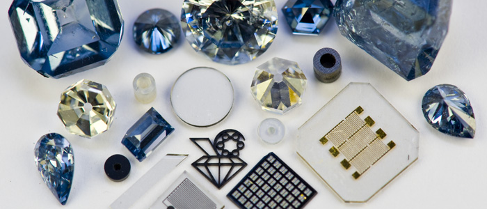
- Developing of technological basis for production of multilayer structures based on synthetic single crystal diamond.
- Development of design of the elements of electronic component base of a new generation high power diamond electronics.
- Research of electrophysical and transport properties of semiconductor synthetic single crystals diamond, in particular under the effect of the optical and ionizing excitation.
- Development of numerical models for calculating the characteristics of electronic devices based on synthetic diamonds.
- Studies of electrical properties of composite nanostructured functional materials, such as thermoelectric alloys doped with fullerene C60 and others.
- Study of nanoscale effects in the new electronic media, such as topological insulators, etc.
Research techniques
- Measuring of electrical resistivity and Hall voltage in the range of 0.1 mohm - 200 Gohm at temperature range of 1.8 K - 800 K and magnetic fields up to 9 T, in particular under the effect of the optical excitation.
- Measuring of the heat capacity and thermal conductivity of solids within the temperature range of 1.8 K - 400 K.
- Measuring of static electrical characteristics of diode and triode structures. Measured voltage range is from 1 nV to 400 V, current range is from 1 fA to 10 A.
- Study of trapping centers in semiconductors structures by methods of the current and capacitance spectroscopy of deep levels with temperature variation from 77 to 800 K.
- Study of the relaxation and transport mechanisms of nonequilibrium charge by measuring the Hall effect under the optical excitation.
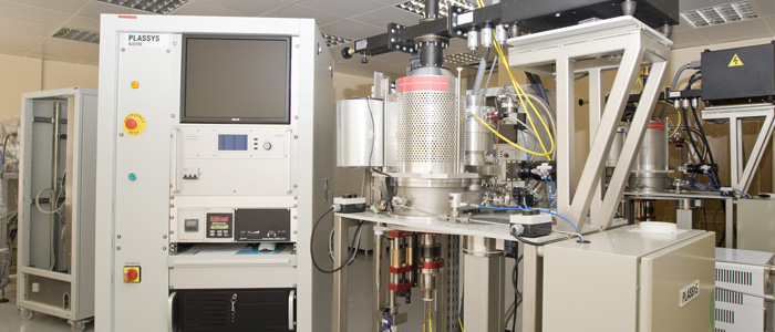
Technological capabilities
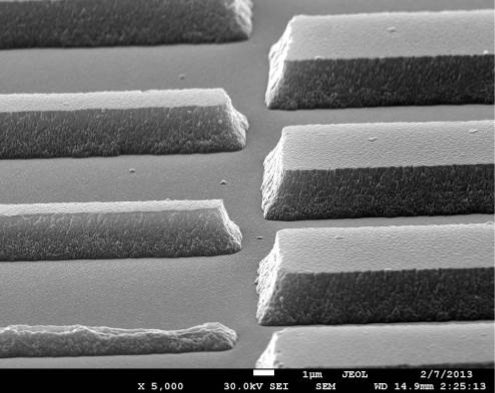
- Formation of contact and dielectric structures by direct and inverse lithography with a minimum element size of 1 micron.
- Magnetron sputtering of metal coatings with controlled thickness in the range from 1 to 1000 nm.
- Deposition of oxide and nitride coatings (including high-k) of thickness under 2 microns by reactive RF sputtering.
- Forming of contact pads by annealing metal and intermetallic coatings to 800 ° C in high vacuum (less than 10-6 Torr).
- Reactive ion etching of semiconductor materials, including synthetic diamond using broad spectrum of gases (Ar, O2, H2, CF4, SF6).
 |
 |
 |
Results obtained
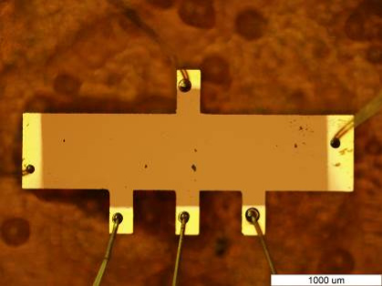
1. The technique of high-speed radiation resistant Schottky diodes based on synthetic single crystal diamonds was developed and mastered.
|
The main characteristics of the diodes: • reverse voltage, Urev • average forward current, Ifw • leakage current at Urev = 1000 V • forward voltage drop at Ifw = 2 A • operating temperature • recovery time |
> 1000 V > 2 A < 100 μA < 4 В from -60 to 250 °С менее 10 нс |
 |
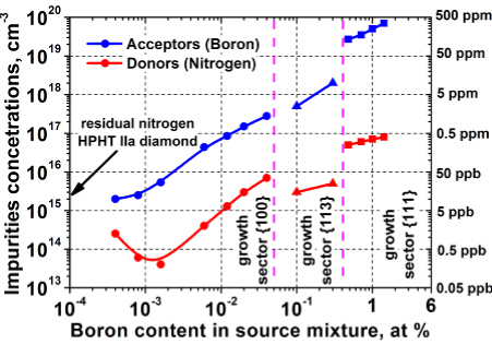
2. The electrical properties of synthetic HPHT single crystal diamonds doped with boron were studied. The relationship between electrical properties and the synthesis parameters were determined. The optimal parameters for synthesis of diamonds for electronic applications were determined.
 |
 |
3. Method of mechanical polishing, cleaning and follow-up quality control of diamond plates for smooth and clean surface suitable for electronic applications was developed.
4. Field transistor model with Schottky gate based on synthetic single crystal diamond was designed.
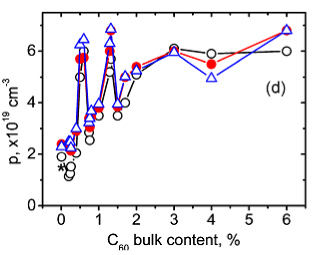
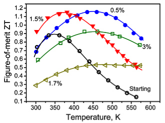
5. The composite nanostructured thermoelectric materials based on a new type of alloys Bi-Sb-Te with fullerene C60 were developed and studied together with the Laboratory of Functional Nanomaterials. Increasing of the thermoelectrics quality factor ZT by 30-70% over a wide temperature range was obtained. The effect of «resonance» concentration of C60 fullerene, with the capture up to 6 electrons to the fullerene molecule, was discovered.
 |
 |
|
Dependence of concentration of free charge carriers (holes) on fullerene C60 concentration in the Bi0.5Sb1.5Te3-C60 alloy |
Dependence of the thermoelectrics quality factor ZT of Bi0.5Sb1.5Te3-C60 alloys on temperature at various concentrations of C60 |
6. Methods of measuring of thermal conductivity and heat capacity of synthetic single crystal diamond in the temperature range of 2 - 400 K was mastered.
 |
 |
 |
 |
Advanced developments on the basis of synthetic diamond
- Solar-blind ultraviolet detectors (wavelength range less then 250 nm), including matrix.
- Dose X-ray and gamma rays detectors, including matrix.
- Spectrometric detectors of ionizing radiation with high energy resolution.
- Countable type detectors for measuring of flux of ionizing radiation.
- Wide range tempreture sensors from 77 to 800 K.
- Acoustoelectric filters, delay lines and microwave resonators.
- Power and high speed Schottky diodes.
- Power and RF FETs.
- Single and broadband microwave generators.
- Elements of RAM.
- independent power supply with a long service life.
Laboratory of Physical Properties of Nanostructures Group of Development and Research of Diamond-based Acoustoelectronic Devices
Group Head Professor, Dr. B. SorokinAcoustoelectronic devices based on bulk (BAW) and surface (SAW) acoustic waves are widely used in creation of acoustic resonators, generators, effective sensors, etc. The group objectives are the development of experimental devices, acoustoelectronic structures, conducting experiments to study the physical properties of crystals and layered structures, modeling propagation of acoustic waves in a crystal, including the conditions of the final external influences.
Research areas
- Development of experimental samples high-overtone bulk acoustic resonators (HBAR), working at 1 – 20 GHz;
- Development of SAW devices based on "IDT/AlN/diamond" layered structure;
- Development of highly sensitive sensors based on acoustoelectronic piezoelectric structures for gas analysis, deposition of ultrathin films, etc.;
- Development of technology for ScxAl1-xN thin piezoelectric films deposition in order to use them in the microwave piezoelectric transducers;
- Study of the acoustic properties of the piezoelectric materials and layered structures and their pressure, temperature, etc. dependences;
- Theoretical and experimental research of microwave attenuation in layered structures, such as "Me1/AlN/Me2/diamond".
Experimental devices
 |
 |
|
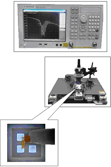
E5071C Vector network analyzer, M-150 workstation, and HBAR testing device |
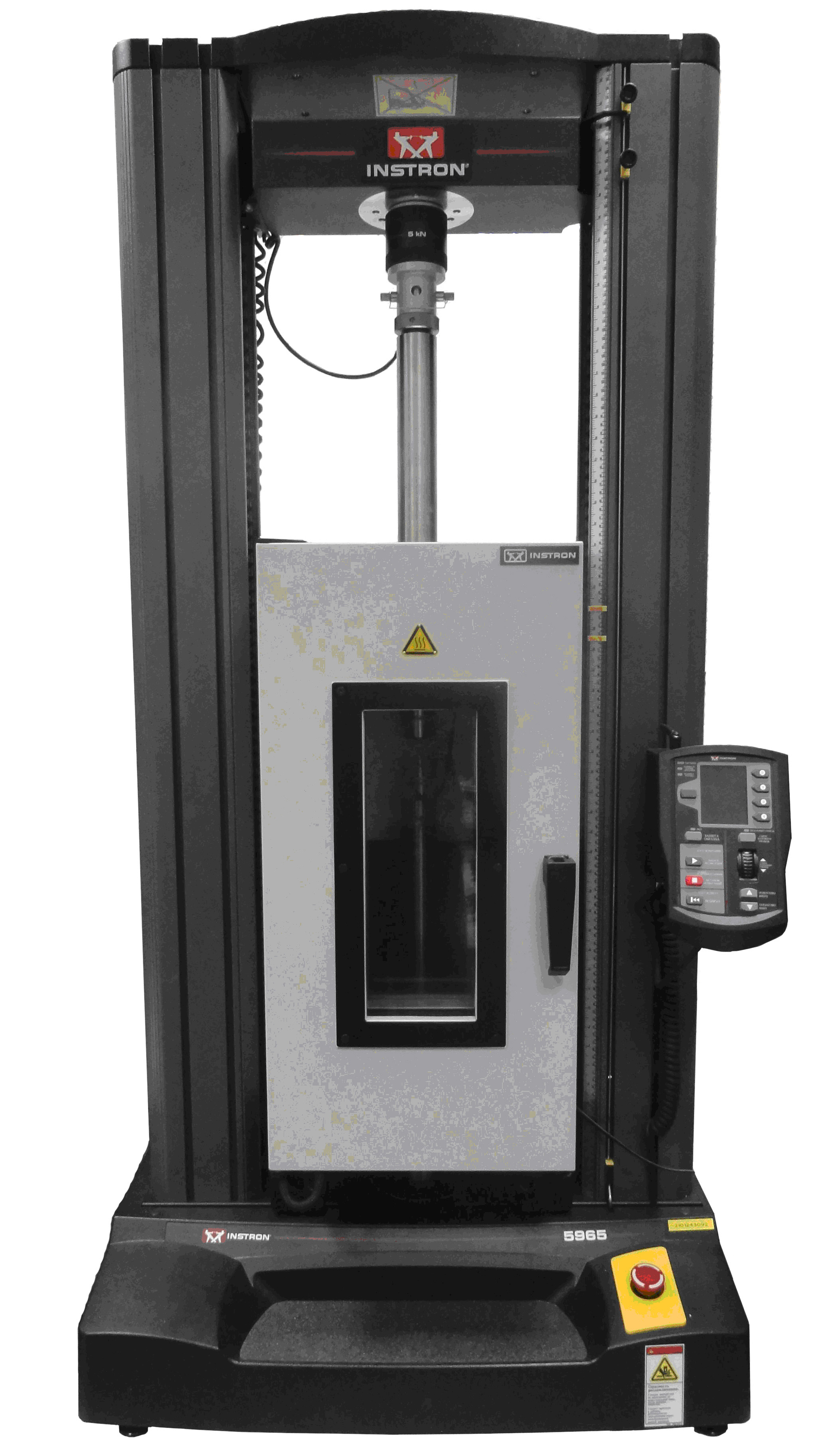
Dual column testing system Instron 5965 for compression with thermal chamber |
Methods
Long pulse method (RAM-5000 installation) is used for measuring acoustic waves velocities in the range of 20-200 MHz with an accuracy of 0.1%. Thin plate samples with a thickness at least 1 mm are used. Acoustic waves are excited by the piezoelectric transducers of X- and Y-cuts of quartz, and 36° and 163° Y-cuts lithium niobate.
Pulse echo method (AVRK-2-B video pulses generator, DPO71254B oscilloscope) used for accurate measurements of the BAW velocities, and their changes due to external influences (pressure, temperature, electric field) in single crystals.
Measurements of AFC, PFC, and other acoustoelectronic devices characteristics are studied by E5071C vector network analyzer and M150 workstation,
working frequency 300 MHz - 20 GHz, temperature range 20 - 300 °C.
Temperature study of acoustic properties of experimental samples produced by Quantum Design installation in the temperature range 4 – 400 °K.
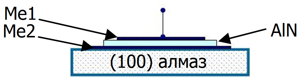
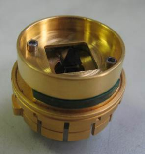
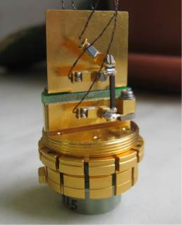
HBAR’s schematic diagram
 |
 |
|
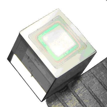
HBAR with a diamond single crystal as a substrate | ||
 | ||
HBAR’s documentation design development in AutoCad |
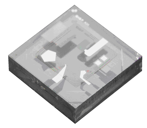
HBAR with a diamond single crystal as a substrate with complex electrodes geometry |

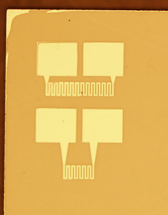
ПАВ резонатор на алмазной подложке.
Резонанс на 418 МГц – ПАВ мода Рэлея (R0),
566 МГц – ПАВ мода Сезавы (R1)
Results
- The second-order elastic constants of IIa type synthetic diamond single crystal were obtained. From measurements of pressure dependences of BAWs velocities for the first time the diamond’s third-order elastic constants were obtained.
- Experimental samples of HBAR with a structure "Me1/AlN/Me2/diamond" were created. The record high resonant frequencies up to 20 GHz and quality parameter Q×f ≤ 105 GHz were obtained. Based on effective data samples pressure and temperature sensors were created.
- Structures characteristics:
• Diamond substrate roughness Ra < 15 nm;
• The accuracy of orientation of the crystallographic faces less than 10’;
• Piezoelectric AlN film thickness from 0.5 to 5.5 μm;
• Metal films thickness from 100 to 300 nm;
• Operation temperature from -100 to +600 °C;
• Operation in the range of uniaxial pressure from 0 to 10 GPa;
• Operating frequencies: 300 MHz - 20 GHz. - Samples of BAW pressure sensors operable at pressures up to 10 GPa were created.
- Experimental samples of SAW resonators and delay lines working on frequencies 400 - 1600 MHz were developed.
- Experimental samples of SAW pressure sensors with a diamond substrate were developed.
Efficient at pressures up to 150 MPa. - SAW and BAW pressure sensors with layered piezoelectric structures based on diamond single crystal have competitive characteristics and can be used for measurements of high and ultrahigh pressures.